
What Is Crucial for the Future of Chip Production
In this section, authors provide their perspectives on economic and financial topics.
Semiconductor manufacturing is not only energy-intensive, but also extraordinarily water-intensive. The fabrication plants) that produce the chips that underpin AI, data centers and modern electronics rely heavily on ultra-pure water (UPW) for rinsing and cleaning as chips are etched on silicon wafers . High-performance chips used in AI models, data center infrastructure and premium smart phones require even more water, pushing the industry’s water demands even higher as they expand.
Unsurprisingly, industry estimates suggest that a single fab can uses roughly 20-38 million liters of water a day – enough to rival the daily consumption of a small city. Large multi-fab sites can exceed this range, particular in hot, water-stressed regions. Taiwan’s chipmaking titan, TSMC, consumed 101 billion liters of water in 2023 alone, with consumption levels rising as next-gen nodes add more layers of circuitry. Those figures rise precipitously when aggregated across the entire industry.
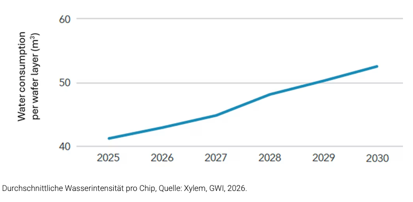
Water intensity of chips continues to rise
Recycling and reclaiming are mission critical
Of course, not all water used in a fab must be ultra-pure. Chip manufacturing relies on multiple grades of water quality for different operations. To reduce external withdrawals from municipal utilities and local watersheds, fabs must reuse water in securely managed loops. For example, UPW, once used, is recycled for use in lower-grade processes such as cooling towers and for wet scrubbing (treating fab exhaust gases). Fabs also ensure that water discharged externally meets strict EPA standards, which are getting more stringent with recent regulations on PFAS and other chemical toxins. Recycling at this intensity and scale requires a full suite of water technologies including: advanced treatment systems to remove particles, metals and other residue; real-time monitoring tools that verify water purity at multiple stages; and special piping to distribute flows whose coatings don’t leach and corrode water streams.
AI and data center growth
In the US, fab growth continues to benefit from the US CHIPS Act which committed USD 39 billion in incentives to reshore and boost semiconductor and advanced manufacturing capacity through 2032.
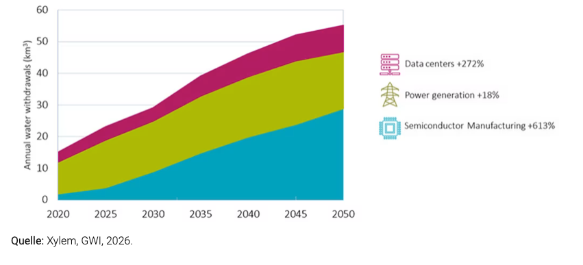
Water demand growth in chip manufacturing and related AI industries
Investment and growth in AI and data centers is not limited to the US. The European Union unveiled the European CHIPS Act, China initiated the third phase of its Integrated Circuit (IC) Industry Investment Fund, and various other incentive programs have emerged in Taiwan, Korea, Japan, India, and around the world. In addition to governments, projected private sector capex totals around USD 2.3 trillion from 2024-2032. According to most assessments, the semiconductor industry was valued in the range of USD 630 billion to USD 680 billion in 2024 and is expected to reach over USD 1 trillion by 2030, largely fueled by the growth of AI and data centers.
Fab location – intensifying the water problem
To make matters worse, semiconductor manufacturing is increasingly concentrated in regions already facing water scarcity. In the US, planned and existing fabs are located in areas that face medium to severe water stress. Globally, critical hubs in Taiwan, South Korea, Singapore, and northern China face similar constraints. A recent analysis found that around 40% of existing semiconductor fabs — and more than 40% of new fabs announced since 2021 — are located in areas projected to face high or extremely high water stress by 2030.
This presents a real operational risk to one of the world’s most strategically important supply chains. Taiwan’s 2021 drought illustrated how water scarcity can disrupt production and force emergency measures (which included trucked in water deliveries). To reduce risks, best-in-class fabs are targeting >70% water recycling and will need even higher levels to operate in droughtprone regions by 2030–2035.
Rising demand requires more utility-scale infrastructure
To combat growing water challenges, leading chip manufacturers are investing heavily in onsite treatment, recycling, and closed-loop water systems. In late 2025, TSMC began construction on a 15-acre industrial water reclamation plant designed to recycle up to 90% of wastewater from its fabs in Arizona’s Silicon Valley. Intel is also spending hundreds of millions on on-site and municipal water infrastructure. It recently partnered with the municipality of Chandler (a Phoenix suburb) to construct the Ocotillo Brine Reduction Facility which will add 11 million liters of treatment capacity to an already sprawling 12-acre on-site water treatment plant. The new facility will support existing fabs, and water infrastructure will expand as additional high-performance fabs are added to the site. Similarly, Samsung is partnering with Korea’s Gyeonggi Province to construct treatment facilities that would enable it use municipal wastewater from five cities for its chipmaking facilities in the area by 2029.
In Germany’s Silicon Saxony, it’s the local authorities who are doing the investing. The EUR 320 million project will ensure uninterrupted supplies of water to the region’s booming semiconductor cluster, whose water demand is expected to significantly increase in the decades ahead. Taiwan’s government is also building a major seawater desalination plant to secure water supplies for Hsinchu Technology Park, a major chipmaking hub, including TSMC fabs. The plant is expected to be finished in 2028 at a cost of EUR 508 million. Hsinchu is part of a national water strategy that will see eight desalination plants constructed to support the nation’s advanced semiconducting manufacturing.
New waves of growth for water companies
This multi-year expansion of fabs translates into demand across multiple segments of the industrial water value chain. Semiconductor water systems rely on complex networks of treatment, purification, cooling, monitoring, and piping and distribution in order to deliver ultrapure water while safely managing contaminated wastewater streams. Large treatment and reclamation plants require advanced membranes, reverse osmosis, and ion exchange technologies to remove particles and dissolved contaminants. Within the fab, additional purification stages produce ultrapure water (UPW) for wafer cleaning, while separate systems manage cooling water used to dissipate heat in facility operations. Continuous monitoring systems track water quality, while specialized pumps, valves, and piping move chemically complex water safely through the facility.
As AI-driven chip production and data infrastructure expand globally, demand is likely to grow across this ecosystem from filtration and purification technologies to water analytics, cooling systems, and industrial flow control solutions.
Amy Wanner-Thavornsuk is Portfoliomanagerin at Robeco.
Read all previous guest contributions here.